Thermal Drift in On-Chip: Photonic crystal sensors (PCS) have gained significant traction in lab-on-a-chip technologies due to their high sensitivity and compact nature. However, one of the fundamental challenges in their deployment is thermal drift, a phenomenon where temperature fluctuations cause changes in the optical properties of the sensor, leading to measurement inaccuracies. This article provides a finite element perspective to analyze thermal drift and proposes potential mitigation strategies.

Photonic crystals (PhCs) are periodic dielectric structures that manipulate light by creating photonic bandgaps, allowing selective filtering of wavelengths. These properties make them highly attractive for biosensing applications. However, variations in temperature induce thermal expansion and refractive index shifts, altering the resonant wavelength of the device. The shift in the refractive index $n$ is governed by the thermo-optic coefficient $(dn/dT)$ of the material, while thermal expansion affects the physical geometry. The combined effect results in a drift of the resonant wavelength $\lambda_r$, which can be expressed as:
$$
\Delta \lambda_r = \lambda_r \left( \frac{1}{n} \frac{dn}{dT} + \alpha \right) \Delta T
$$
where $\alpha$ is the thermal expansion coefficient. For high-index contrast materials like silicon, the thermo-optic coefficient dominates, leading to redshifts in resonance peaks with increasing temperature.
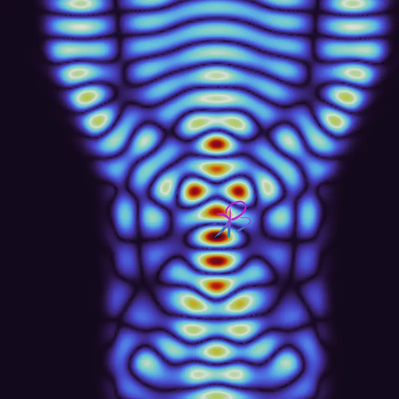
To quantify this drift, finite element simulations are conducted using software such as COMSOL Multiphysics. The model typically consists of a 2D or 3D periodic photonic crystal slab, where heat transfer equations are coupled with electromagnetic wave propagation using the finite element method (FEM). The governing heat diffusion equation:
$$
\rho C_p \frac{\partial T}{\partial t} = \nabla \cdot (k \nabla T) + Q
$$
describes the temperature distribution across the photonic crystal, where $\rho$ is the density, $C_p$ the heat capacity, $k$ the thermal conductivity, and $Q$ the heat source. This temperature field is then linked to Maxwell’s equations:
$$
\nabla \times \left( \frac{1}{\mu} \nabla \times \mathbf{E} \right) - \epsilon_r \frac{\partial^2 \mathbf{E}}{\partial t^2} = 0
$$
to determine the shift in resonance wavelength. Results from FEM simulations typically show a linear relationship between temperature and wavelength shift, with redshifts of 80-100 pm/K for silicon-based photonic crystals.
Mitigation Strategies
Several approaches can be employed to reduce thermal drift. One effective strategy is the use of thermally compensated designs, where a secondary material with a negative thermo-optic coefficient is integrated. Materials like silicon nitride (SiN) or polymers with lower thermo-optic coefficients can counterbalance silicon’s positive $dn/dT$. Additionally, introducing thermal isolation trenches in the photonic chip can localize heat dissipation and reduce unwanted thermal crosstalk. Active feedback loops using temperature sensors and tuning mechanisms, such as micro-heaters, can further stabilize the sensor response.
Experimental Validation
Recent studies have demonstrated the feasibility of these strategies. For instance, experiments with hybrid Si-SiN photonic crystal cavities have shown a 50% reduction in thermal drift compared to silicon-only structures. Similarly, integrated microfluidic cooling systems have been employed to maintain temperature stability, particularly in biosensing applications where precision is critical.
Thermal drift poses a significant challenge in photonic crystal sensors, affecting their accuracy and reliability. A finite element approach provides an invaluable tool for predicting and mitigating these effects. By employing thermally compensated materials, isolation structures, and active feedback mechanisms, the impact of temperature fluctuations can be significantly reduced, paving the way for highly stable on-chip photonic sensing solutions.
Reference:
thermal drift on a polymeric photonic crystal slab sensor
Fiber-tip photonic crystal for real-time
Slow-light-enhanced on-chip 1D and 2D photonic crystal
Discussions? let's talk here
Check out YouTube channel, published research
you can contact us (bkacademy.in@gmail.com)
Interested to Learn Engineering modelling Check our Courses 🙂
All product names, trademarks, and registered trademarks mentioned in this article are the property of their respective owners. Use of these names does not imply any affiliation, endorsement, or sponsorship. The views expressed are those of the author and do not necessarily represent the views of any organizations with which they may be affiliated.
