Photonic crystal nanocavities (PCNCs) have revolutionized the field of integrated photonics by enabling ultra-high quality factor ($Q$) resonators for various applications, including optical sensing, nonlinear optics, and quantum information processing. The design and optimization of high-$Q$ photonic crystal nanocavities require advanced computational modeling techniques, among which Finite Element Analysis (FEA) stands out due to its ability to handle complex geometries, boundary conditions, and material dispersions.
Finite Element Analysis is a numerical method used to solve Maxwell’s equations in photonic structures by discretizing the domain into small elements. This technique is particularly suitable for photonic crystal nanocavities, where high precision is needed to capture mode profiles, cavity resonances, and quality factors accurately. FEA allows the computation of the electromagnetic field distribution within the cavity, enabling precise determination of resonant wavelengths and loss mechanisms.
The design of a high-$Q$ nanocavity typically involves engineering defect modes in a periodic photonic crystal lattice. The introduction of localized defects within a two-dimensional photonic crystal slab can create a resonant mode that is confined due to Bragg reflection and total internal reflection. The $Q$-factor of such cavities is defined as:
$$
Q = \frac{\omega_0}{\Delta\omega}
$$
where $\omega_0$ is the resonant frequency, and $\Delta\omega$ is the full-width at half-maximum (FWHM) of the resonance peak. A higher $Q$-factor indicates lower energy dissipation and improved sensitivity, making these cavities ideal for on-chip sensing applications.
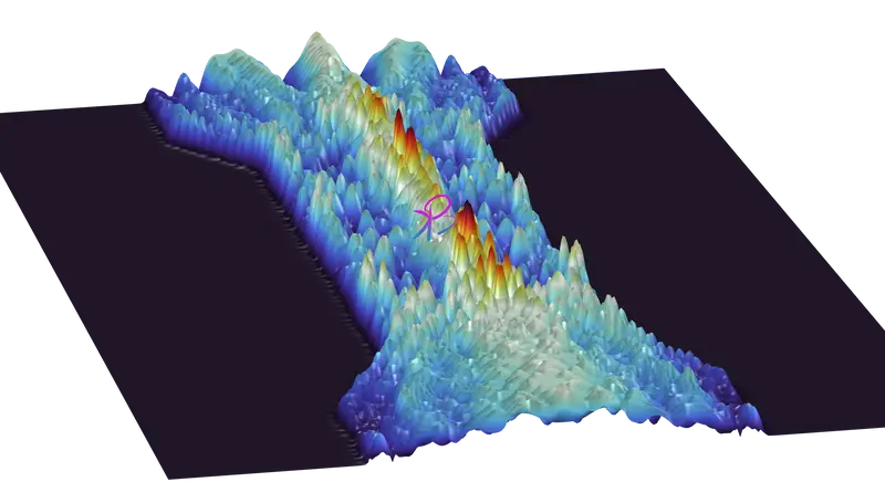
One of the key challenges in modeling photonic crystal nanocavities is minimizing computational errors due to boundary conditions. Typically, Perfectly Matched Layers (PMLs) or Bloch-Floquet periodic boundary conditions are used to prevent artificial reflections and simulate an open-domain environment. In FEA, meshing plays a critical role in achieving accurate solutions. A finer mesh in regions of high field confinement ensures the precise calculation of cavity resonances and mode profiles.
Material dispersion is another crucial factor influencing the cavity performance. In high-index contrast materials such as silicon-on-insulator (SOI) platforms, the dispersion relation must be accurately modeled to predict the shift in resonance wavelengths due to environmental perturbations. The inclusion of thermo-optic and nonlinear effects further enhances the applicability of these cavities in sensing applications.
For on-chip sensing, the sensitivity of a nanocavity is quantified by its wavelength shift per unit refractive index change ($S = \Delta\lambda / \Delta n$). Higher-$Q$ cavities exhibit stronger light-matter interactions, leading to enhanced sensitivity. The integration of photonic crystal nanocavities with microfluidic channels allows real-time biosensing by detecting minute changes in the refractive index of the surrounding medium. This principle has been successfully applied in label-free biosensors for detecting biomolecules, viruses, and chemical analytes.
Recent advancements in FEA-based modeling have enabled the optimization of cavity geometries to achieve $Q$-factors exceeding $10^6$, pushing the limits of photonic crystal-based sensing. Computational techniques such as adjoint-based optimization and machine learning-assisted inverse design are now being used to refine cavity designs beyond conventional approaches.
Finite Element Analysis provides a powerful framework for the design and analysis of high-$Q$ photonic crystal nanocavities. By leveraging advanced numerical techniques, researchers can develop next-generation on-chip sensors with ultra-high sensitivity and selectivity. The integration of these cavities with lab-on-chip platforms opens new avenues for applications in biomedical diagnostics, environmental monitoring, and quantum photonics.
For further exploration, refer to recent works in photonic crystal cavity optimization and computational photonics modeling:
Analysis of high-Q photonic crystal
On-chip spectroscopy with thermally tuned high-Q photonic crystal cavities
Ultrahigh-Q photonic crystal nanocavities
Discussions? let's talk here
Check out YouTube channel, published research
you can contact us (bkacademy.in@gmail.com)
Interested to Learn Engineering modelling Check our Courses 🙂
All product names, trademarks, and registered trademarks mentioned in this article are the property of their respective owners. Use of these names does not imply any affiliation, endorsement, or sponsorship. The views expressed are those of the author and do not necessarily represent the views of any organizations with which they may be affiliated.
