Finite Element Analysis (FEA) plays a crucial role in optimizing the integration of photonic crystal (PhC) sensors with silicon photonics. This integration is fundamental for advancing optical sensing technologies used in biomedical applications, environmental monitoring, and high-speed optical communication. Photonic crystals, with their periodic dielectric structures, exhibit unique light-manipulation properties, such as photonic bandgaps, that enable high sensitivity to changes in their surrounding environment. However, coupling these sensors efficiently with silicon photonic waveguides presents significant challenges due to mismatches in mode profiles, impedance, and fabrication constraints.
FEA enables precise modeling of the electromagnetic field distribution in photonic crystal structures and silicon waveguides. By solving Maxwell’s equations in a discretized computational domain, FEA provides insights into mode propagation, scattering losses, and coupling efficiencies. The method is particularly effective in optimizing interface designs, such as tapered waveguides, grating couplers, or mode-matching layers, which improve light transmission between PhC sensors and silicon photonics. The effectiveness of these interfaces is measured by transmission efficiency, insertion loss, and modal overlap, all of which can be rigorously analyzed using FEA-based simulations.
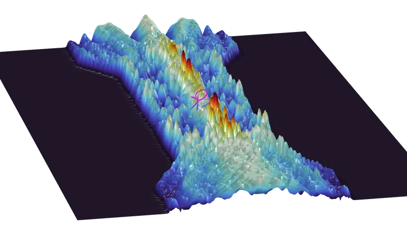
One of the primary advantages of FEA in this domain is its ability to handle complex geometries with high precision. Photonic crystal cavities, which enhance light-matter interactions through high-Q resonances, require precise structural tuning for optimal performance. Any minor deviation in hole size, lattice constant, or refractive index can significantly impact sensor performance. FEA allows researchers to predict and mitigate these effects by simulating various fabrication imperfections and environmental conditions, such as temperature variations and material dispersion.
Another critical aspect where FEA excels is in optimizing the placement of photonic crystal sensors within a silicon photonic circuit. For instance, in biosensing applications, a PhC sensor can be integrated into a silicon waveguide to detect minute refractive index changes caused by biomolecular interactions. The sensitivity of such a setup depends on the evanescent field overlap between the silicon waveguide mode and the PhC defect mode. FEA provides a numerical framework to study these interactions and refine the design to achieve the highest possible sensitivity.
Beyond passive coupling, FEA also plays a role in active tuning mechanisms, such as thermo-optic and electro-optic modulation, which are essential for dynamically reconfigurable photonic systems. By incorporating material-dependent thermal and electronic properties into the simulations, FEA helps in designing PhC-based tunable filters and sensors that can operate at different wavelengths or adapt to changing environmental conditions.
Recent research studies have demonstrated the effectiveness of FEA in this field. For example, a study published in Optics Express showed that optimized silicon-to-PhC coupling structures based on FEA simulations achieved coupling efficiencies exceeding 90% while minimizing insertion loss. Similarly, a report in Nature Photonics highlighted how FEA-assisted design improvements led to high-Q photonic crystal cavities for single-molecule detection. These case studies underline the indispensable role of FEA in pushing the boundaries of integrated photonic sensing technologies.
FEA-driven design methodologies continue to evolve, incorporating machine learning and inverse design techniques to further refine photonic crystal sensor integration. By leveraging FEA, engineers and researchers can systematically explore design spaces that were previously inaccessible due to computational constraints. As silicon photonics moves towards mass production for consumer and industrial applications, the precise control enabled by FEA will be critical for ensuring repeatability and performance reliability in photonic crystal-based sensing systems.
Basic calculations
The integration of photonic crystal sensors with silicon photonics requires an in-depth understanding of light propagation and coupling mechanisms. This is governed by Maxwell’s equations, which form the foundation for electromagnetic field analysis. In the context of finite element analysis (FEA), these equations are solved numerically over a meshed computational domain. The core governing equations for time-harmonic electromagnetic fields in a non-magnetic, source-free medium are given by:
$$
\begin{aligned}
\nabla \times \mathbf{E} &= -j\omega\mu_0 \mathbf{H}, \\
\nabla \times \mathbf{H} &= j\omega\varepsilon(\mathbf{r}) \mathbf{E},
\end{aligned}
$$
where $\mathbf{E}$ and $\mathbf{H}$ represent the electric and magnetic field vectors, $\omega$ is the angular frequency, $\mu_0$ is the permeability of free space, and $\varepsilon(\mathbf{r})$ is the position-dependent permittivity of the photonic structure.
To quantify the efficiency of light coupling between a photonic crystal defect mode and a silicon waveguide, the mode overlap integral is a crucial parameter, defined as:
$$
\eta = \frac{\left| \int_{\Omega} E_{\text{PhC}}^* \cdot E_{\text{Si}} \, dA \right|^2}{\int_{\Omega} |E_{\text{PhC}}|^2 \, dA \int_{\Omega} |E_{\text{Si}}|^2 \, dA}
$$
where $E_{\text{PhC}}$ and $E_{\text{Si}}$ are the electric field distributions of the photonic crystal mode and the silicon waveguide mode, respectively. The integration is performed over the overlap region $\Omega$. A high value of $\eta$ indicates efficient coupling with minimal scattering losses.
In practical implementations, a photonic crystal cavity coupled to a silicon waveguide introduces a strong resonance effect, leading to high-Q factor modes. The quality factor $Q$ of such a cavity is given by:
$$
Q = \frac{\omega_0}{\Delta \omega} = \frac{2\pi f_0 U}{P_{\text{loss}}},
$$
where $\omega_0 = 2\pi f_0$ is the resonant frequency, $\Delta \omega$ is the linewidth of the resonance, $U$ represents the stored electromagnetic energy, and $P_{\text{loss}}$ accounts for radiative and material losses. High-Q resonators are crucial in sensing applications, as they enhance the interaction of light with the surrounding medium, thereby improving detection sensitivity. Moreover, the coupling efficiency between a silicon waveguide and a photonic crystal structure can be optimized using impedance matching principles. The effective impedance of the photonic crystal region, $Z_{\text{PhC}}$, is derived from the Bloch mode expansion:
$$
Z_{\text{PhC}} = \frac{E_x}{H_y} = \sqrt{\frac{\mu_0}{\varepsilon_{\text{eff}}}},
$$
where $\varepsilon_{\text{eff}}$ is the effective permittivity of the photonic crystal structure. A gradual impedance transition via tapered structures or graded-index metamaterials helps in achieving impedance matching, reducing reflection losses, and enhancing coupling efficiency. These mathematical models are important to understand for FEA simulations, allowing engineers to optimize photonic crystal-silicon photonics integration. By refining structural parameters such as lattice constant, hole radius, and waveguide width, FEA-driven designs can achieve near-ideal coupling conditions, paving the way for high-performance photonic sensors and communication devices.
For further reading on the latest advancements in photonic crystal-silicon photonics coupling, refer to Optics Express and Nature Photonics.
Discussions? let's talk here
Check out YouTube channel, published research
you can contact us (bkacademy.in@gmail.com)
Interested to Learn Engineering modelling Check our Courses 🙂
All product names, trademarks, and registered trademarks mentioned in this article are the property of their respective owners. Use of these names does not imply any affiliation, endorsement, or sponsorship. The views expressed are those of the author and do not necessarily represent the views of any organizations with which they may be affiliated.
